|
||||
| News and Information about the Test of Electronics in Research & Design, Production, Maintenance, and Installation. | ||||

Main MenuNewsletterNews AreaInfo AreaWeblinksProduct Focus |

Readers Top 5 News of last 30 days
Latest Test and Measurement NewsWafer MVM-SEM Tool supports Next-Generation Devices
It is a stable, high-accuracy measurement solution for process development at the 1Xnm node and mass production at the 22nm node and beyond, contributing to reduced process TAT (turn around time) and higher productivity. The E3310 will be featured in Advantest’s exhibit (booth #3D-803 in Hall 3) at the SEMICON Japan trade show, December 5-7 in Makuhari Messe in the Chiba prefecture. A Next-Generation 3D Measurement Solution While advances in semiconductor technology have historically followed Moore’s Law, technical challenges have recently imperiled the transition to yet-smaller processes. The development of 3D transistor technologies such as FINFET (fin-based field effect transistors) is expected to bridge the gap to mass production at the 22nm node and subsequently the 1Xnm node. Advantest’s new E3310 provides a stable, highly accurate 3D measurement solution suitable for these next-generation needs. Product Features 3D Measurement The E3310’s multi-detector configuration allows it to achieve stable, highly accurate measurements at the 1Xnm node. It also features a proprietary detection algorithm, enabling measurement of the 3D FinFET architectures that are in the process of full-scale adoption by the semiconductor industry. Highly Stable, Fully Automatic Image Capture The E3310 performs stable, fully automatic measurements even at high SEM magnification, thanks to its high-accuracy stage, charge control function, and contamination reduction technology. Support for Diverse Wafer Types Not only silicon wafers, but AlTiC, quartz, and silicon carbide wafers, among others, are supported in sizes from 150mm to 300mm, depends on type. www.advantest.comRelated Articles: |

Upcoming Events More events...
Tag CloudOscilloscope
JTAG
Boundary Scan
Goepel
PXI
Rohde & Schwarz
Tektronix
Keysight
AOI
Anritsu
National Instruments
Inspection
Teledyne LeCroy
Aeroflex
LTE
Yokogawa
AXI
Spectrum Analyzer
Keithley
In-Circuit-Test
Signal Analyzer
Automotive
EMC-Test
Signal Generator
Advantest
Multitest
B&K Precision
Corelis
Power Supply
SPI
Flying Prober
Teseq
Cognex
Switching
Teradyne
Viscom
Pickering
Fluke
GAO Tek
PCIe
|
||
|
© All about Test 2018 |
||||
 How to resolve AdBlock issue?
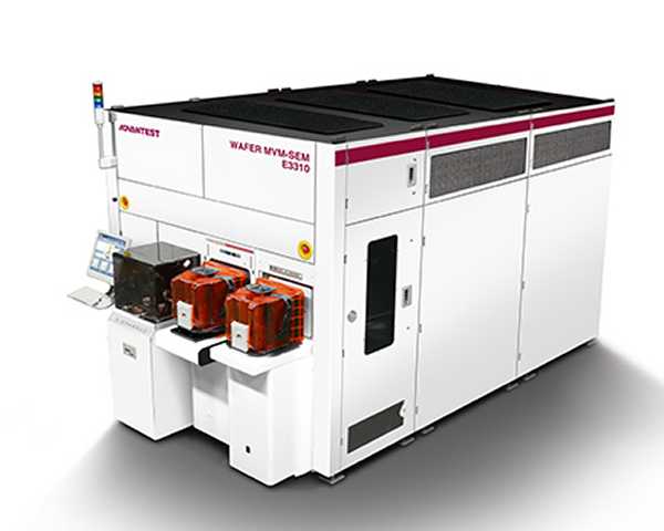 26 November 2012 - Advantest has introduced its new Multi-Vision Metrology Scanning Electron Microscope, the Wafer MVM-SEM E3310, which measures fine-pitch patterns on a wide range of wafer types with unparalleled accuracy, utilizing Advantest’s proprietary electron beam scanning technology. Built on advances in the technology used in Advantest’s E3630 MVM-SEM for photomasks, the E3310 achieves superior capabilities for scanning and measurement of wafers for next-generation devices.