 |

Main Menu
Newsletter
News Area
Info Area
Weblinks
Product Focus

 How to resolve AdBlock issue?
 Readers Top 5 News of last 30 days
- 27 March 2024 - GPP 5G Conformance Test Solutions with small Footprint
- 03 April 2024 - 5-in-1 Programmable Oscilloscopes
- 05 April 2024 - Oscilloscope Days event in April 2024
- 28 March 2024 - RF Test Enclosures provide highly-isolated Bench-top Environments
- 11 April 2024 - Flying Probe Tester for Probe Cards
News - Component Test
Innovative Wafer Inspection combining 2D and 3D Measurements
 02 December 2013 - Since the density and complexity of wafer structures increase every year, the industry needs high-performing and reliable systems for quality control. Against this background, ISRA VISION introduces a product line offering an innovative technological approach for non-contact optical wafer inspection. As required, different 2D and 3D gauging procedures may be combined into one inspection system measuring structure sizes of down to 1 micrometer in under one minute.
This means that several wafer analyses may be performed in the FEOL process at the same location. As a consequence, defects in material and structure can be identified early in the process, opening up the possibility to eliminate damaged wafers - an efficient approach to reducing costs.
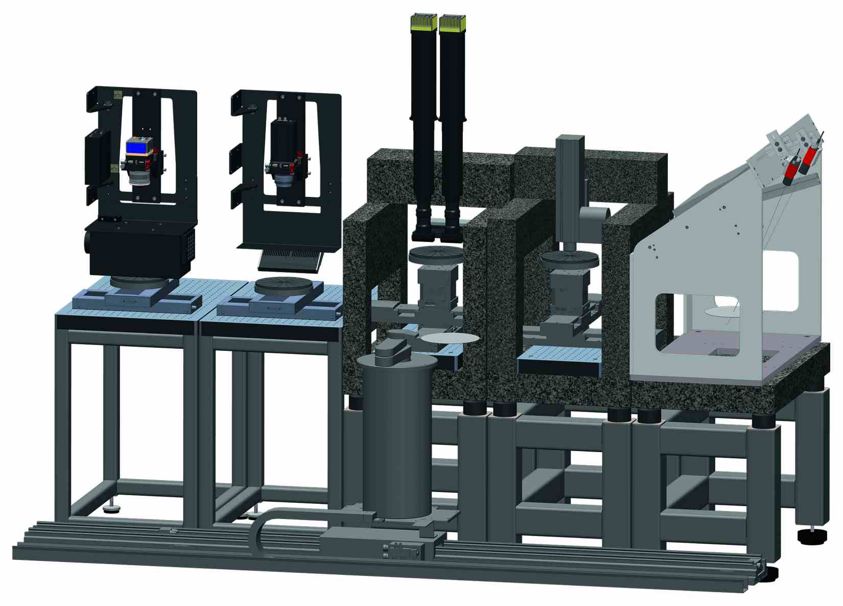
ISRA provides an inspection system which allows to be composed of different components according to customer requirements. It can be used along the entire process chain from the wafer input through the front-end-of-line (FEOL) to the back-end-of-line (BEOL) and ensures the quality of silicon, gallium arsenide and sapphire wafers with diameters of up to 8 inches. The modules also cover partial processes such as after-development inspection, shallow-trench isolation and chemical mechanical planarization (CMP). The technology is SEMI-compliant and suitable for clean room usage.
Free space is valuable in production facilities. ISRA therefore gives users a choice of combining inspection modules in compact clusters. In this way, several measurements may be made at one place. For example, the inspection technology offers a pattern recognition function during the FEOL process stage as it is required for the MEMS sensor technology: It is possible to measure vertical structure profiles in the sub-µ range in less than 1 minute in order to rule out possible production defects and tolerances. In the cluster, a debris check with an accuracy of down to 20 micrometers may be added. At the same time, an RGB color analysis with a resolution of 20 micrometers may be applied, which is unique on the market in this respect. It supports the detection of defects and surface modifications such as oxide layers, diffusion layers and color changes.
Another innovation is the inspection of unstructured wafers with regard to their topography by means of phase-measuring deflectometry at further line positions. With a resolution in the range of nanometers, bows or warpages can be safely identified. In the particular case of high-current applications, it is essential to locate hidden microcracks in wafers. ISRA's technology uses a resolution of 80 micrometers and hence detects even the finest inside cracks.
The combination of high-resolution 2D inspection, RGB multi-spectral analysis and 3D white-light interferometry allows for the implementation of flexible customized solutions. Customers may freely choose among the modules and compile an individual cluster meeting their requirements. Each module, however, can also be operated as a stand-alone solution.
Conclusion: So far, procedures such as UV laser, e-Beam or X-ray have been applied for wafer quality control, but are significantly more expensive and require complex installations. The innovative semi-conductor technology by ISRA represents an unprecedented, inexpensive and efficient tool for high-resolution structure analyses of wafers.
Related Articles:

Upcoming Events
More events...
See our Trade Show Calendar
Click here
Tag Cloud
© All about Test 2018