 |

Main Menu
Newsletter
News Area
Info Area
Weblinks
Product Focus

 How to resolve AdBlock issue?
 Readers Top 5 News of last 30 days
- 27 March 2024 - GPP 5G Conformance Test Solutions with small Footprint
- 21 March 2024 - Stackable High Voltage Measurement Modules
- 22 March 2024 - Decode, Trigger & Search Support for the CAN XL Protocol
- 25 March 2024 - Debug and Trace Support for new Arm Automotive CPUs
- 03 April 2024 - 5-in-1 Programmable Oscilloscopes
News - Component Test
Die-Level Handling System for KGD Test Strategy
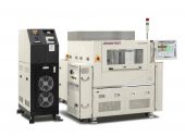 14 June 2016 – Advantest Corporation introduced its HA1000 die-level handler, a cost-efficient test solution for determining known good dies (KGD) prior to IC packaging. The HA1000 is designed to handle a wide variety of devices from large high-power server/GPU type devices to small system-on-chips (SoCs) and memory devices/stacks, such as HBM2.
Economics is a driving factor in die-level testing. Determining a semiconductor device’s viability prior to packaging or building memory stacks is critical to avoiding rework, achieving high yields and lowering costs. Performing pre-assembly testing of singulated devices provides a new level of visibility into the quality of the device prior to committing additional devices and expensive packages to an assembly which could potentially have to be scrapped because of undetected problems. Advantest’s new die level handler allows full device testing to be performed before assembly, providing time-critical information that today is typically only available at final test.
“Testing and debugging today’s 2.5D, 3D and fine-pitch chip-scale-package devices require a KGD approach capable of testing the ICs while they are still in die form,” said Zoë Conroy, manager, Silicon Test and Product Engineering, Technology and Quality, Supply Chain Operations of Cisco Corporation. “Using the HA1000 to do KGD testing has enabled a faster time-to-market, lowering the overall product cost.”
Koichi Tsukui, senior vice president at Advantest Corporation commented, “We have leveraged knowledge stemming from decades of experience in device handling and thermal control technology to develop this new class of die-level-handlers. Our customers can now precisely position and probe singulated devices after they have been bumped, thinned and sawed. They will realize improved yields at final assembly, and that is an important achievement.”
Advantest’s HA1000 is designed to handle a wide variety of devices from large high-power server/GPU type devices to small system-on-chips (SoCs) and memory devices/stacks, such as HBM2. The die-level-handler can handle thick parts and thin parts as well as stacks of 3D devices and partially or fully assembled 2.5D integrations. In addition, the HA1000 is ideal to probe fine-pitch pads, bumps, microbumps and pillars. Future applications of the system may also include the probing of Through-Silicon-Vias (TSVs).
The handler employs a precision vision alignment system capable of precisely positioning probe points to the finest pitch in use today. While properly positioning the chuck under the probes, the system can also adjust the planarity to match with the device surface to insure a solid device connection.
An active thermal control (ATC) system enables the HA1000 to adjust on the fly to temperature fluctuations at the die’s surface over a very broad dynamic range of -40˚ C to 125˚ C. The temperature of the thermal head quickly responds using a hot-cold fluid mix. Thanks to low thermal resistance and high thermal capacity the system can handle high power devices with a thermal responsiveness which is often better than is possible in a packaged environment. This allows manufactures to test parts at higher power levels and/or tighter margins which can improve yields while reducing scrap.
Production units of the new HA1000system have already begun shipping.
www.advantest.de/
Related Articles:

Upcoming Events
More events...
See our Trade Show Calendar
Click here
Tag Cloud
© All about Test 2018