 |

Main Menu
Newsletter
News Area
Info Area
Weblinks
Product Focus

 How to resolve AdBlock issue?
 Readers Top 5 News of last 30 days
- 27 March 2024 - GPP 5G Conformance Test Solutions with small Footprint
- 03 April 2024 - 5-in-1 Programmable Oscilloscopes
- 05 April 2024 - Oscilloscope Days event in April 2024
- 28 March 2024 - RF Test Enclosures provide highly-isolated Bench-top Environments
- 11 April 2024 - Flying Probe Tester for Probe Cards
News - Component Test
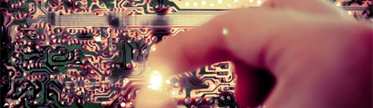
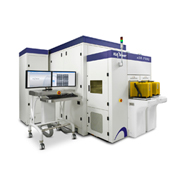 Electron-Beam Wafer Defect Review System
23 August 2011 - KLA-Tencor Corporation announced a critical enabling tool for chip manufacturing at the 20nm device nodes and below: the eDR-7000 electron-beam (e-beam) wafer defect review system. Featuring technology breakthroughs that produce industry-leading sensitivity and throughput, the eDR-7000 addresses defect imaging and classification challenges at today's leading edge—where yield-killing defects can be as small as 10nm, or located at the bottom of a deep trench or hole.
Referring to KLA-Tencor the eDR-7000 is the only tool in its class to reliably identify defects down to the sensitivity thresholds of wafer defect inspection systems designed for the 20nm node. These include the Surfscan SP3, introduced last month, and KLA-Tencor's upcoming models in the patterned wafer inspection product lines.
"The eDR-7000 offers the opportunity to thoroughly understand the defect population on the wafer," said Cecelia Campochiaro, Ph.D., vice president and general manager of KLA-Tencor's e-Beam Technology division. "This new tool is able to re-locate and image 10nm defects and defect types that are typically missed by currently available review systems. It can review multiple defects per second —primarily because it can drive directly to the site of the defect at high resolution, without having to take the intermediate, time-consuming step of locating the defect at lower magnification, and then zooming in for a clear image. With the outstanding quality and quantity of data afforded by the eDR-7000, engineers are equipped to take appropriate corrective action based on an accurate representation of the defect population."
The leading-edge capabilities of the eDR-7000 are enabled by the following new features and improvements over the current-generation eDR-5210 platform:
Third-generation, field-tested e-beam immersion column, for higher resolution and improved topographic imaging;
Advanced stage and vibration-isolation system, for a three-fold improvement in coordinate accuracy and up to a four-fold increase in defect review speed;
Dramatically improved sensitivity to defects on bare wafers, including enhancements to energy-dispersive x-ray (EDX) composition analysis;
Unique reticle defect review mode, for rapid investigation of sites on the wafer where reticle defects may have printed;
Process window characterization at significantly greater throughput;
Voltage-contrast imaging mode for review of e-beam wafer inspection data; and
Offline defect classification capability to increase the tool's availability for imaging work.
Several orders have been received for eDR-7000 systems from leading logic, memory, foundry, and equipment manufacturers. Multiple systems are already in use in advanced development and production lines.
www.kla-tencor.comRelated Articles:

Upcoming Events
More events...
See our Trade Show Calendar
Click here
Tag Cloud
© All about Test 2018