 |

Main Menu
Newsletter
News Area
Info Area
Weblinks
Product Focus

 How to resolve AdBlock issue?
 Readers Top 5 News of last 30 days
- 03 April 2024 - 5-in-1 Programmable Oscilloscopes
- 05 April 2024 - Oscilloscope Days event in April 2024
- 28 March 2024 - RF Test Enclosures provide highly-isolated Bench-top Environments
- 11 April 2024 - Flying Probe Tester for Probe Cards
- 02 April 2024 - Advantest appointed new Group CEO
News - Component Test
Advantest launches Photo Mask Measurement Tool
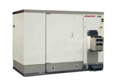 27 November 2013 - Advantest Corporation launched its new E3640 MVM-SEM (Multi Vision Metrology Scanning Electron Microscope) tool for measurement of patterns on photomasks and other media ad dimensions as small as 1Xnm. A new entry in Advantest’s widely-adopted E3600 Series of SEM systems, the E3640 delivers significantly improved measurement accuracy and higher throughput. Its industry-best pattern measurement capability supports the coming shift to the 1Xnm node for semiconductor volume production.
In addition to photomasks for standard semiconductor lithography, the E3640 also offers enhanced metrology performance for EUV masks, NIL templates, and patterned media.
Amid rising demand from the mobile device segment of the end-user market, the semiconductor industry is expected to shift mass production to the 1Xnm process in the near future. This shift will stimulate new requirements for stable, highly accurate pattern dimension measurement at these extremely small scales. The E3640 satisfies these requirements with industry-leading precision measurement capabilities and upgraded functionality that enhances mask R&D and production efficiency.
The E3640 is scheduled to be available from June 2014. It will be exhibited at Advantest’s booth at SEMICON Japan 2013, to be held on December 4-6, 2013, at Makuhari Messe, near Tokyo.
Related Articles:

Upcoming Events
More events...
See our Trade Show Calendar
Click here
Tag Cloud
© All about Test 2018